Nikon Z6 Camera Overview
Nearly two months ago, we dove into the Nikon Z7 and showed you what was happing inside all the way down to the sensor. Today, we did the same with the Z7’s standard resolution counterpart, the Nikon Z6. At 25 megapixels and just under $2000 MSRP, the Z6 is encroaching on the Sony A7 III’s turf. The A7 III has proven itself to be a high-performing, tuned down version of the A7R III, “the basic model”, delivering beyond what the market is accustomed to at that price point. So, does the Z6 meet this new standard for the $2000 camera body? The specs certainly check out, but what about the build? Is the Z6 as well built as the Z7, or did Nikon cut corners to meet the lower price point?
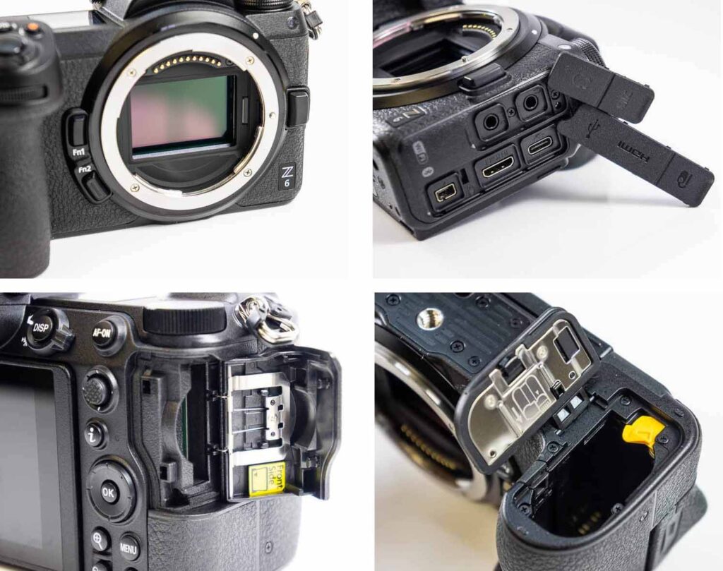
Nikon Z6 Build Quality and Z7 Comparison
Cosmetically, the Z6 is identical to the Z7 if you don’t count the little ‘6’ in the lower right-hand corner of its front panel. The two bodies are exactly the same weight, gram for gram. All the exterior sealing is there where it was on the Z7, and the body is incredibly solid with no rattling, jingling, or play between the parts. The differences between the Z6 and Z7 are purely internal.
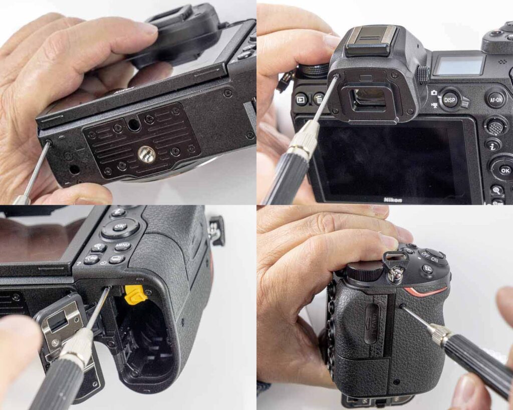
Starting the Nikon Z6 Teardown
Disassembly begins much the same way as the Z7 as well. The outer screws are in the same places, there are still quite a few of them, and the battery retention clip will still fire out of the bottom of the camera at great speed if you’re not careful.
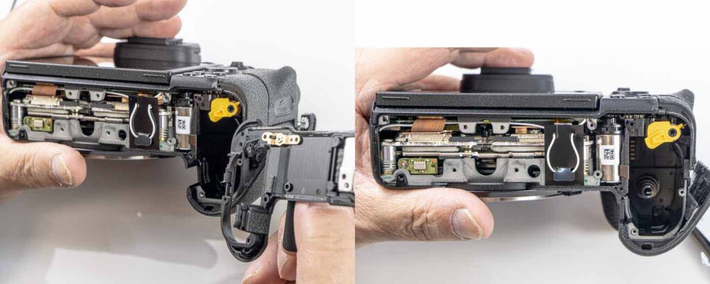
Opening the Camera Body and Rear Panel
The bottom will come off first. It’s quite cramped in there with very little empty space, unlike the EOS R. The sensor stabilization mechanism dominates the internals of the camera and sits on some hefty springs.
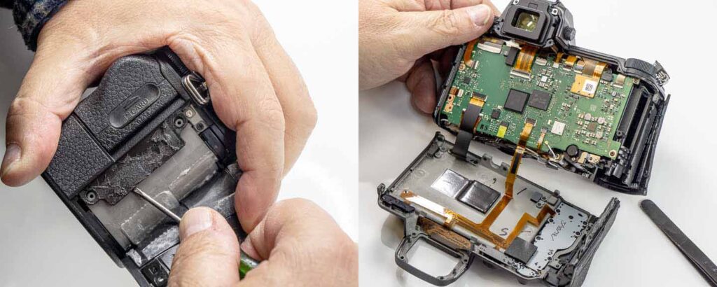
With some peeling, prying, and good ol’ fashioned elbow grease, the back panel and LCD will come off in one piece, exposing the motherboard.
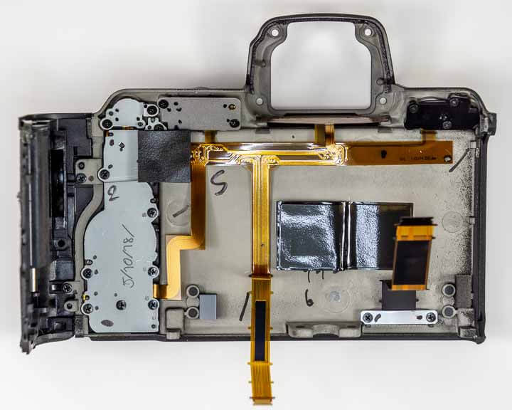
Motherboard Layout and Ribbon Cable Connectors
A look at the back panel. There isn’t much to see here, and that’s probably a good thing. Neatly arranged cables and a modest amount heat sinking material are not only pleasant for us as technicians, but they also suggest careful design and good temperature control, something that has been an issue for Sony cameras.
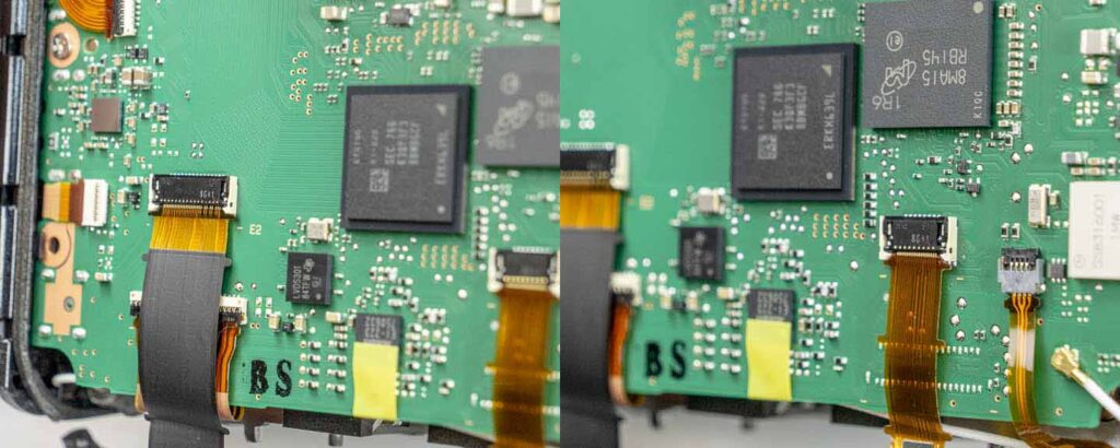
Taking a closer look at the board, we see a new type of ribbon cable connector that we first encountered inside the Z7.
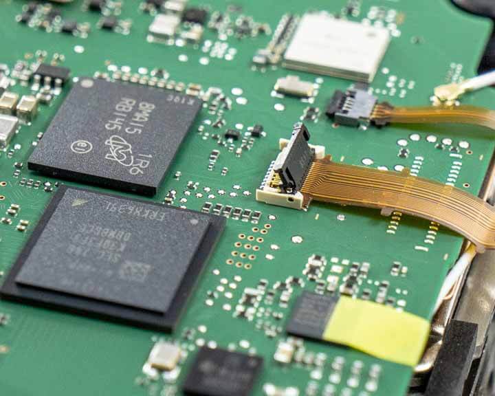
Here’s a closeup of one of them in action.
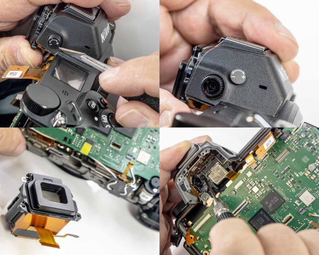
Removing the EVF Screw and Main Board
Before the main board can come out, a screw underneath the EVF has to come out. For the EVF to come out, you need to remove a screw hidden underneath the viewfinder diopter dial. These new mirrorless cameras are tricky to take apart. The latest generation Sony cameras have a similar arrangement.
Now, you can remove the screws holding the board in place and flip it up and out of the camera. Don’t forget to unhook all connections, of course. (As you can see here, we did things slightly out of order. As I said above, these new mirrorless cameras are tricky to get apart.)
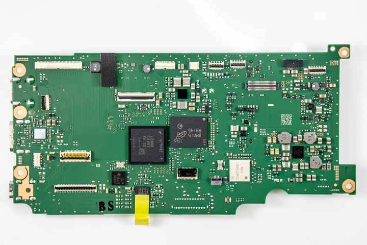
Here is the motherboard in all its glory. Take a closer look and let us know if you see anything interesting in the comments.
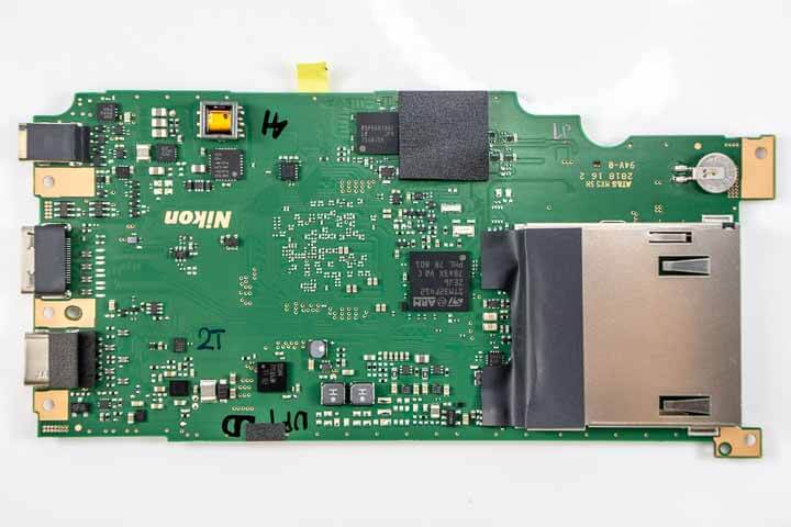
And the flip side, featuring a single XQD card reader.
Removing the Nikon Z6 Sensor and IBIS Assembly
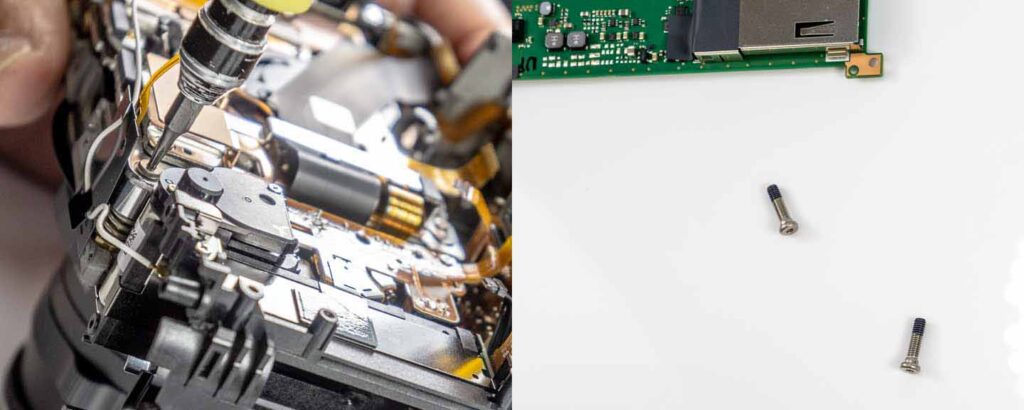
Now that the board is out of the camera and in a safe place, we can extract the exceptionally hefty screws holding the sensor assembly on its exceptionally hefty springs. Just look at the size of these guys.
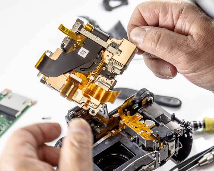
Now you’re free to extract the sensor and IBIS shaker mechanism and raise it up proudly like a newborn child.
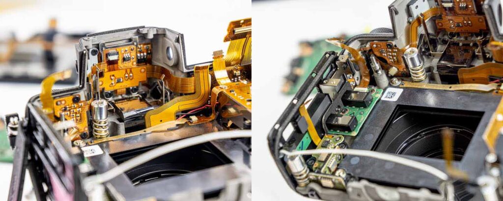
Some closeup views of what lies beneath the sensor before we move on. The input and output audio jacks are quarantined on their own separate board, another feature shared by Sony. This design makes it far more acceptable for them to get wet or damaged. If they do, they probably won’t short out the entire motherboard like they might if they were integrated onto that crucial part.
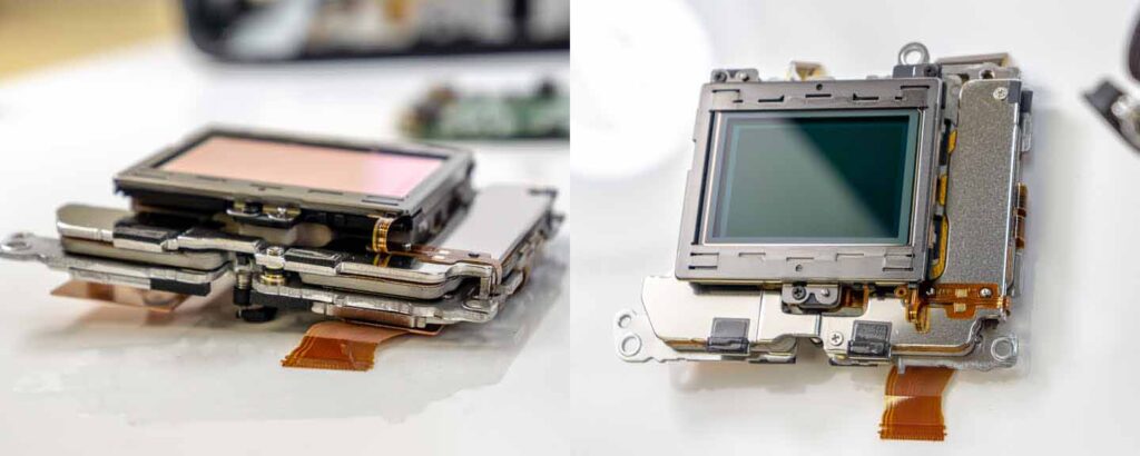
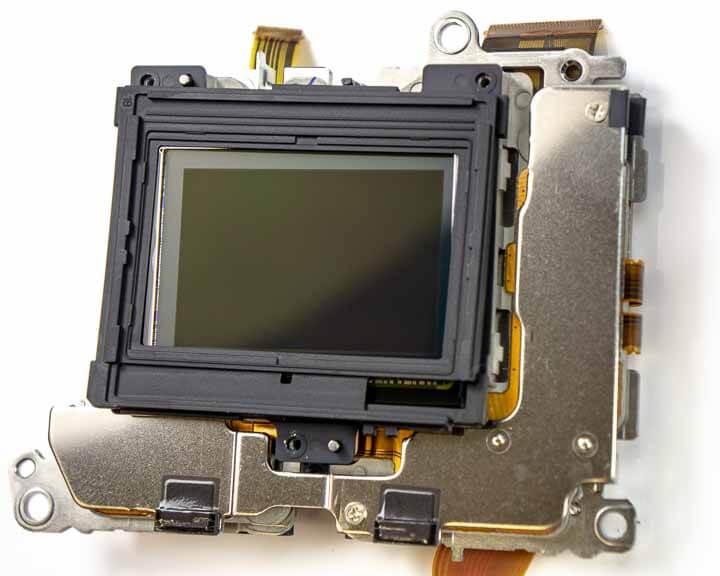
The Nikon Z6’s sensor is certainly no less of a behemoth than the Z7’s, either. If it has 21 fewer pixels of resolution, you certainly can’t tell by looking at it. (Disclaimer: This was a joke. Please don’t feed me into a woodchipper in the comments section for saying that.) Another thing we noticed was how stiff the IBIS shaker seemed compared to those found in other cameras. It barely budges when pressure is applied, but it still boasts the same 5 stops of stabilization claimed by the A7 III.
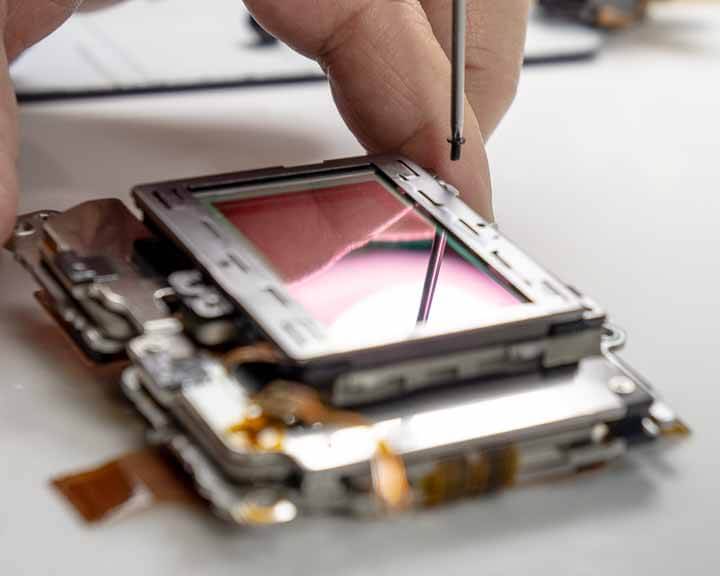
Nikon Z6 Sensor Glass and Thin Filter Conversion Potential
Now for our specialty: the glass in front of the sensor.
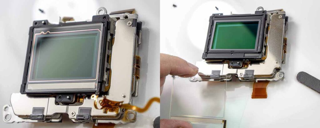
The dust reduction system glass measures in at a bit over 0.3mm thick.

The lowpass IR/UV cut filer underneath is thicker, at 0.8mm. This puts the total thickness of the Nikon Z6’s sensor glass at 1.1mm, identical to the Z7. This makes the Z6 an excellent candidate for adapting legacy film and rangefinder lenses. However, our Ultra-Thin conversion, measuring in at 0.2mm, is still the best option of optimal legacy lens performance with a mirrorless digital camera. (Coming soon for the Nikon Z series)
Nikon Z6 Internal Design and Final Thoughts
So, what does this mean for the Great Mirrorless Camera War as its first year draws to a close? The Nikon Z6 and Z7 are of identical build quality as well as construction as far as we could tell from the extent of our disassembly. Nikon follows the example set by Sony in some aspects of its design as well as it’s market philosophy. The cameras also improves upon the Sony A7 series in certain areas like cover glass thickness, weather sealing, and heat management. However, as we previously discussed, neither the Sony or Nikon cameras come close to the Canon EOS R in terms of beautiful design, and that’s a fact. Each full frame mirrorless camera so far has had its relative strengths and weaknesses. 2018 is leaving us in a stalemate. Perhaps, with the big three major brands no longer playing catch-up, 2019 will bring more decisive developments to this conflict.



6 Responses
Neither the Sony or Anon cameras come close to the Niko Z6/7 in terms of beautiful design, and that’s a fact.
Agreeed
No that’s your opinion!
Thanks for another interesting tear-down. How does the weather sealing compare to the Z7, identical? I believe that was superior.
This is an awesome Tutorial!
The Z6 motherboard looks nearly identical to the Z7.